
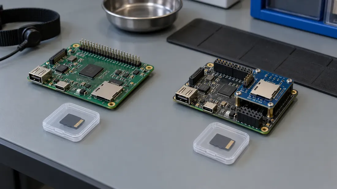
microSD SPI vs Native SD Bus Mode: Interface Differences and Throughput Limits
- SPI mode is a secondary protocol subset selected during the initial reset sequence, operating over a single data line.
- SD speed class markings do not give a guaranteed throughput figure for a particular SPI host.
- Host SPI clock limits, firmware block sizing, and protocol command overhead heavily dictate real-world transfer rates.
When integrating microSD cards into embedded host systems, hardware and firmware engineers must choose between the legacy Serial Peripheral Interface (SPI) mode and the native SD bus mode. The SD Association (SDA) Physical Layer Specification defines SPI as an alternate communication protocol designed for lower-complexity hosts, but the trade-offs in interface complexity, protocol overhead, and transfer rates are significant.
Mode Selection and Protocol Architecture
According to the SDA Physical Layer Specification, a card defaults to native SD bus mode upon power-up. SPI mode is selected when the host asserts the Chip Select (CS) line low while sending the reset command (CMD0). Once placed in SPI mode, the card remains in this state until a complete power cycle occurs.
Native SD mode provides a dedicated command line (CMD) and scalable data lines (DAT0–DAT3), supporting negotiated bus modes such as Default Speed (up to 25 MHz) and High Speed (up to 50 MHz), with higher UHS signaling defined for compatible cards and hosts. In contrast, SPI mode operates as a byte-oriented protocol over standard MOSI, MISO, SCK, and CS lines, lacking the advanced handshaking, wider bus widths, and multi-line signaling of native SD.
Speed Class Applicability in SPI
A common misconception is that a card's marked speed class rating (such as Class 10, UHS Speed Class 3, or Video Speed Class V30) guarantees a minimum sequential write speed in SPI mode.
The SD Association speed class guidance relates markings to supported bus modes and defined test conditions. It does not supply a guaranteed transfer rate for an arbitrary SPI implementation. Measure the actual card and host together.
Interface Comparison
| Feature / Parameter | SPI Mode | Native SD Mode (1-bit / 4-bit) |
|---|---|---|
| Data Bus Width | 1-bit (MOSI/MISO) | 1-bit (DAT0) or 4-bit (DAT0–DAT3) |
| Interface Selection | Selected at first reset (CMD0 with CS low) | Default power-on state |
| Speed Class Marking | No direct throughput promise for the tested SPI host | Depends on the card class and a compatible native bus mode |
| Comparison needed | Host SPI clock, command pattern and firmware | Negotiated bus mode, clock and host/card capability |
Host Factors Influencing Real-World Throughput
Because card capabilities vary and not all cards support all native advanced modes, real-world throughput depends heavily on host-level parameters:
- Host SPI Clock Frequency: Record the actual stable clock configured on the target board; no universal microcontroller limit applies.
- Transfer Pattern: Record whether the software uses single- or multiple-block transfers and the amount of work per command.
- Firmware Buffering: Check whether host buffering or other work interrupts transfers.
- Board Implementation: Use the exact host design and signal-integrity limits to determine the stable clock; do not infer a wiring defect from one throughput result.
Validation Recording Checklist
When benchmarking storage throughput across hardware revisions, record:
- The active interface mode (SPI, 1-bit native SD, or 4-bit native SD).
- Host bus clock frequency and duty cycle.
- The command sequence used (e.g.,
CMD17/CMD24vs.CMD18/CMD25). - File system cluster size and memory buffer allocation per transfer.
For a candidate card, include the host mode, clock and measured workload in a quote request.
References
We publish measured usable capacity and define trial-batch verification against the quoted product and agreed test scope.